Home-English etc.
English Home
Participation of SIF in SEMICON West 2013, seeking partners and Rep.

Carrier Integration Inc. are approved to paticipate SIF poster session in SEMICON West 2013.
Session is held on July 9th,2013.
--------------------
Offering Multi-Sized Wafer Processing including 450mm Process Development and Control
Carrier Integration Inc. is prepared with launching 450mm carriers in 4 structures to offer to semiconductor equipment manufactures and semiconductor wafer manufacturers for characterization of device and process parameters as well as parameters distribution in 450mm wafers.
Carrier Integration Inc. hopes to extend its availability to U.S. and worldwide customers through local representative in U.S. and for this purpose it is seeking to find willing partners and /or sale representatives as well as investors in this operation.
The candidate of representatives is who has experience in semiconductor equipment sales and has been sevicing with strong network to key
persons of equipment manufacturers and wafer manufacteres.
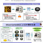
Good News about cost down of compound semiconductor & all other devices !!!
New technology has released for compound semiconductor process with different materials and sizes, so called "Silicon carrier" and "Process integration" on it.
Carrier Integration Inc. is a new venture company established on December 10th, 2010. Our product is, however, an application product of semiconductor general-process technology which has been under researched and developed by AIST(the National Institute of Advanced Industrial Science and Technology) since 2004. The base of the technology was demonstrated at the field of lithography in AIST in 2007, for the first time. Then, developed to many other fields, such as annealing,bonding,ethching,deposition and measurement.
By using our product , Silicon Carrier (SC), as the New BridgeTool, an existing silicon device manufacturing equipment can be used for a process of compound semiconductor devices without any modification. Our products, "Silicon Carrier(SC)", are relaized by the high-tech of precise machining at μm resolution. As you know, an existing machine for silicon device processing needed to be modified if you want to process a compound semiconductor because a wafer of compound semiconductor is small (1 to 5 inch). By using a SC, you can do process for small size of samples with different shape, it is very useful for compound semiconductors, such as SiC, GaN ,InP and GaAs.
Now we have started to accept an order of Silicon Carrier.
Please contact to us with your request, we will provide solutions of SC, with customer's satisfaction.
About our fellow subsidiary
Wafer Integration Inc. is established as on December 10th, 2010, and authhorized as a venture company from AIST in 2011. Wafer Integration Inc. has been demonstrated "Nano Probe Technology" for Direct and Precise characterization of nano-integrated circuits, which bring new scopes for advanced integrated circuits, "which can measure the characteristics of transistors by probing directly onto the semiconductor devices." Click here to the Home Page!